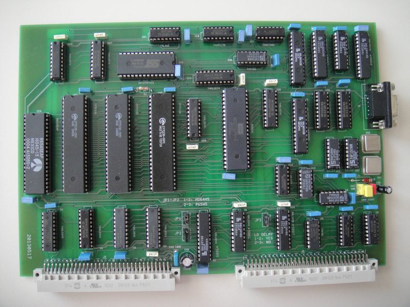
Text Only VGA Board
Text-VGA Board with R6545EAP
Schematics:
Part 1 of 5 - BUS & Line Driver
Part 2 of 5 - Timing & Wait Generator
Part 3 of 5 - CRTC & I/O
Part 4 of 5 - Video RAM
Part 5 of 5 - Shift Reg. & RGBI Output
Accessing video-RAM
One of the problems in the design of a video card is: how to efficiently access video ram?
The CRTC accessed sequentially video ram, gradually increasing the generated address.
The CPU accesses the video ram when he occasionally need to change the appearance of the screen.
The most intensive operation that the CPU has to do is scrolling the screen.
The CPU can not access the video memory during the CRTC accesses, otherwise do not get a good screen quality.
The CRTC needs access to the memory only during the portion of time in which its clock (character clock = CCLK) is high.
Uswing for the CPU a PHI2 = inverted CCLK the problem is fully resolved, and both devices have uniimpeded access to the video memory.
But how do when CCLK and PHI2 are unrelated? A possible solution is to synchronize the CPU access to the video RAM so that this takes
place only during the time in which CCLK is at low level.
This can be achieved with the following basic circuit:
Basic circuit for video ram access
The timing diagram of the circuit showing the operation of the circuit (Simulation performed with the module OrCad VST):
Timing diagram
Note that:
CCLK is character clock to CRTC
PHI2 is CPU clock
/LD is the load signal for shift register
/VRM is the access video ram signal generated by CPU (via a decoder)
RDY is the "ready" signal to CPU
/WR1 and /WR2 are two signal can be used to write (or read) the video ram
During a write cycle the CPU will be stopped, vith data bus "frozen", then a write cycle to the memory can be easily done
with one of the two signals and /WR1 or /WR2 (my favorite is /WR1).
During a read cycle, it is necessary to use a latch (driven by one of the two signals and /WR1 or /WR2), in such a way that
at the end of the cycle the CPU can correctly sample the data bus and fetch the byte from memory.
Using a dual-port RAM as video ram the latch for reading don't longer need. Also by this way can be eliminated the mux. for
address lines (the mux can be driven by /WR2 signal). This is the solution used in the video card presented here.
In this way, the CPU must be stopped only during the write cycles, but not during read cycles.